TSMC News.
8 stories in the last 7 days
Everything TSMC across dozens of tech sources, distilled by AI into sharp ~100-word summaries and updated hourly. Follow TSMC to pin its stories to your For You feed. Tap any story for the full brief, or open the original source.
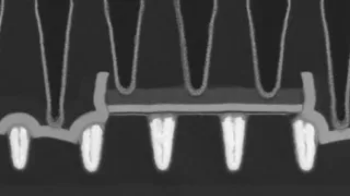
Imec, ASML, and TSMC integrated n-type and p-type 2D-material transistors on a single 300mm wafer at a 50nm contacted poly pitch, the tightest demonstrated for complementary 2D devices. 94% of transistors switched correctly with an on/off current ratio above 100,000. The work narrows the gap on p-type 2D CMOS performance.

Taiwan Semiconductor (TSM) dominates advanced chip manufacturing with FY2026 revenue forecast at $163.8B, a 27.5% increase from prior estimates. Surging AI and data center demand drive growth. Robust free cash flow, margin expansion, and a $106B cash position justify a continued bullish rating despite elevated valuation multiples.
Samsung Foundry has received orders or is in negotiations with Google, Nvidia, Tesla, AMD, and BYD for sub-5nm chips. Some of these companies previously worked exclusively with TSMC but are now engaging with Samsung due to TSMC's demand struggles.

Samsung receives increased advanced chip requests from BYD, Google, and AMD as TSMC faces AI-driven capacity limits. The demand surge pressures TSMC's manufacturing output. Samsung's chip production capacity is being utilized more heavily in 2026.

TSMC and Amkor Technology announced a long-term partnership to accelerate advanced semiconductor packaging in the United States. The collaboration aims to expand domestic packaging capacity and strengthen the supply chain for advanced chips.
TSMC stated at its European Technology Symposium that panel-level packaging will not replace wafer-level CoWoS for large AI processors. Wafer-level technology can scale to integrate 58 massive dies in one package. Panel-based processes lack the interconnection density of wafer-level tech, according to senior vice president Kevin Zhang.

TSMC is advancing chip packaging technologies to close the gap on Samsung's current packaging advantages. The move focuses on improving density and thermal performance in mobile and AI chips. Industry analysts say TSMC's new 3D stacking process could enable faster, more power-efficient devices.

TSMC is developing CoPoS (Chip-on-Panel-on-Substrate) packaging, shifting from wafer-based to panel-level processing. The technology reduces manufacturing costs and supports larger packages for AI accelerators. Mass production is expected in the second half of 2028. CoPoS will complement, not replace, existing CoWoS packaging.
Summaries by ByteBrief